Understanding the Manufacturing Processes Behind Step Gold Finger PCBs
2024-06-05
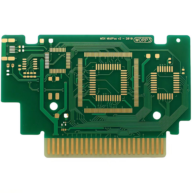
In the world of electronics, the intricacies of printed circuit boards (PCBs) often go unnoticed, yet they form the backbone of countless devices we rely on daily. Among the specialized types of PCBs, the Step Gold Finger PCB stands out due to its unique structure and enhanced functionality. But what exactly goes into manufacturing these sophisticated components? Let's dive into the specific processes involved in the production of a Step Gold Finger PCB.
1. Design and Layout
The journey of creating a Step Gold Finger PCB begins with meticulous design and layout. Engineers utilize advanced CAD (Computer-Aided Design) software to draft the PCB's schematics, ensuring all components are accurately placed. This stage involves defining the exact locations and dimensions of the gold fingers—those crucial connectors that interface with other devices or components.
2. Substrate Preparation
The substrate, typically made from a material like FR4 (a type of fiberglass), serves as the foundation of the PCB. The substrate undergoes thorough cleaning to remove any contaminants that could interfere with the subsequent layering processes. This preparation ensures a pristine surface for the application of conductive materials.
3. Layering and Lamination
Once the substrate is ready, it’s time to add the conductive layers. This is usually done through a lamination process where layers of copper are bonded to the substrate under high pressure and temperature. For multi-layer Step Gold Finger PCBs, multiple cycles of layering and lamination may be required to build up the necessary number of layers.
4. Drilling and Plating Through Holes
Next, precise holes are drilled into the laminated substrate to accommodate component leads and vias (connections between different layers). After drilling, these holes are plated with copper to establish electrical connectivity. This step is critical for the overall functionality of the PCB, ensuring that signals can travel seamlessly through the board.
5. Etching
The etching process defines the circuitry on the PCB. A photoresist material is applied to the copper surface and exposed to UV light through a mask that represents the circuit design. The exposed areas are then developed, leaving behind a pattern that protects certain areas of copper. The unprotected copper is etched away using a chemical solution, revealing the desired circuit paths.
6. Applying the Solder Mask and Silkscreen
After etching, a solder mask is applied to insulate the copper traces and prevent short circuits during soldering. This is followed by the application of a silkscreen layer, which provides labels and markings to help with component placement and identification. Both layers are crucial for the assembly and functionality of the PCB.
Conclusion
The production of a Step Gold Finger PCB is a complex, multi-step process that requires precision and expertise at every stage. From design and substrate preparation to gold plating and quality control, each step is meticulously carried out to ensure the final product meets the highest standards of performance and reliability. Understanding these processes not only highlights the sophistication behind modern electronics but also underscores the importance of quality manufacturing in delivering dependable technology.